Saturday, August 15, 2026

old yeller

© 2026 Bryan R. Hinton
Provenance · Integrity Record
Hashes are of the byte-identical images converted from raw sensor data. Verify with sha512sum -c SHA512SUMS.
Fingerprint: CA42 47E8 9A5E FEAB 36DC 6A42 C547 9171 B69A 3CFB 887D B92C 3FB1 480A 2993 57A3
The .ots file proves that SHA512SUMS existed at or before the Bitcoin block timestamp below.
Anchor: Bitcoin block 962622
Timestamp: 2026-08-15 20:04 UTC
SHA512SUMS.ots

Friday, August 14, 2026

Eastern Grip

Some chains just hold the bike. Others hold the memory.
© 2026 Bryan R. Hinton
Provenance · Integrity Record
Hashes are of the byte-identical images converted from raw sensor data. Verify with sha512sum -c SHA512SUMS.
Fingerprint: CA42 47E8 9A5E FEAB 36DC 6A42 C547 9171 B69A 3CFB 887D B92C 3FB1 480A 2993 57A3
The .ots file proves that SHA512SUMS existed at or before the Bitcoin block timestamp below.
Anchor: Bitcoin block 962481
Timestamp: 2026-08-14 21:59 UTC
SHA512SUMS.ots

Majdanek

Mausoleum, State Museum at Majdanek. This is a primary record of my visit.
© 2026 Bryan R. Hinton
Provenance · Integrity Record
Hashes are of the byte-identical JPEGs converted from raw sensor data. Verify with sha512sum -c SHA512SUMS.
Fingerprint: CA42 47E8 9A5E FEAB 36DC 6A42 C547 9171 B69A 3CFB 887D B92C 3FB1 480A 2993 57A3
The .ots file proves that SHA512SUMS existed at or before the Bitcoin block timestamp below.
Anchor: Bitcoin block 962233
Timestamp: 2026-08-13 03:55 UTC
SHA512SUMS.ots

Across from Where She Stood

This side of the canal.
© 2026 Bryan R. Hinton
Provenance · Integrity Record
Hashes are of the byte-identical JPEGs converted from raw sensor data. Verify with sha512sum -c SHA512SUMS.
Fingerprint: CA42 47E8 9A5E FEAB 36DC 6A42 C547 9171 B69A 3CFB 887D B92C 3FB1 480A 2993 57A3
The .ots file proves that SHA512SUMS existed at or before the Bitcoin block timestamp below.
Anchor: Bitcoin block 962351
Timestamp: 2026-08-14 00:28 UTC
SHA512SUMS.ots

Wednesday, August 12, 2026

Aktenvermerk: Konvergenz am Ort

During my visit to the Jüdisches Museum Frankfurt am Main, I photographed this decorative plaque bearing the Schma Israel ("Hear, O Israel") — the central prayer of Jewish faith. Inscribed in both Hebrew and German, it was designed to hang on the eastern wall of a synagogue, facing Jerusalem. Its imagery is rich with Temple symbolism: the two columns represent the twelve tribes of Israel, crowned lions frame a radiant medallion with the name of God, and below sits the Ark of the Covenant, which once held the tablets of the law in the Holy of Holies.

What struck me was how a single object could distill so much - faith, history, exile, and longing for Jerusalem, into one visual composition. While similar plaques sometimes appeared in homes as Mizrah indicators of prayer direction, this particular piece was clearly made for a synagogue, as its formal design and Temple references suggest.

This plaque is a remnant of a German Jewish community that was nearly annihilated during the Shoah. Today, it survives as a witness – both to what was built and to what was lost.

A small but powerful reminder of the depth of German Jewish heritage.

Jüdisches Museum Frankfurt Am Main.  Schmuckblatt mit dem Gebet Schma Israel (Höre Israel). Personally photographed by me at Jüdisches Museum Frankfurt Am Main. This is a primary record of my visit. © 2026 Bryan R. Hinton
Provenance · Integrity Record
Hashes are of the byte-identical JPEGs converted from raw sensor data. Verify with sha512sum -c SHA512SUMS.
Fingerprint: CA42 47E8 9A5E FEAB 36DC 6A42 C547 9171 B69A 3CFB 887D B92C 3FB1 480A 2993 57A3
The .ots file proves that SHA512SUMS existed at or before the Bitcoin block timestamp below.
Anchor: Bitcoin block 951258
Timestamp: 2026-05-27 07:49 UTC
SHA512SUMS.ots

Wednesday, July 8, 2026

Places of Memory · Kraków, Poland

Kraków, Poland
© 2026 Bryan R. Hinton
Provenance · Integrity Record
Hashes are of the byte-identical JPEGs converted from raw sensor data. Verify with sha512sum -c SHA512SUMS.
Fingerprint: 2969 AEB8 0A42 E021 5E66 4D93 BD9B C85E 0213 8166 415C 9171 2074 3657 B386 AF51
The .ots file proves that SHA512SUMS existed at or before the Bitcoin block timestamp below.
Anchor: Bitcoin block 951191
Timestamp: 2026-05-27 00:49 UTC
SHA512SUMS.ots

Friday, May 29, 2026

A thousand years on Polish soil

 Cienin. Jeszcze w cieniu Majdanka.
© 2026 Bryan R. Hinton

Between five and six million Polish citizens were murdered, three million of them Polish Jews. Much of the killing was carried out on that same soil: at Auschwitz-Birkenau, Treblinka, Sobibór, Bełżec, Majdanek, and Chełmno, all of them Nazi German camps and killing centers built in occupied Poland. Whole towns where no one came home. A civilization of a thousand years, destroyed in five.

The ideologies behind these crimes do not disappear by themselves. Each generation must carry that weight, and act on it.

The fields look ordinary now. The forests have grown back. The track is still there.

What remains is the duty to remember precisely. The names. The places. The dates. The silence in those places now is not empty. It is the shape of what was taken.

This is a shared history, and it cannot be told without Poland. For nearly a thousand years, from the Statute of Kalisz in 1264 through the academies of Kraków and Lublin, the printing houses of Warsaw, and the streets of Wilno, Polish Jews built one of the great civilizations of Europe. They were Polish citizens. They wrote in Polish, in Yiddish, and in Hebrew. They fought in Polish uprisings. They are buried in Polish soil.

To study this history through the objects, documents, and testimonies that preserve it, I recommend:

POLIN Museum of the History of Polish Jews
Warsaw

OÅ›rodek „Brama Grodzka – Teatr NN”
Lublin

Emanuel Ringelblum Jewish Historical Institute
Żydowski Instytut Historyczny, Warsaw

Provenance · Integrity Record
Hashes are of the byte-identical JPEGs converted from raw sensor data. Verify with sha512sum -c SHA512SUMS.
Fingerprint: 2969 AEB8 0A42 E021 5E66 4D93 BD9B C85E 0213 8166 415C 9171 2074 3657 B386 AF51
The .ots file proves that SHA512SUMS existed at or before the Bitcoin block timestamp below.
Anchor: Bitcoin block 951191
Timestamp: 2026-05-27 00:49 UTC
SHA512SUMS.ots

Thursday, May 28, 2026

KL Auschwitz-Birkenau · The Outer Perimeter

Auschwitz II-Birkenau
© 2026 Bryan R. Hinton

This is a photo that I took while walking around Auschwitz II-Birkenau in Oświęcim, Poland. The camp is huge. The barracks in the distance are to the left of the barracks where Edith Frank, Anne Frank, and Margot Frank supposedly stayed. Otto stayed at Auschwitz I.

I reached my arm through the fence to take this photo. It was a very important day.

Provenance · Integrity Record
Hash is of the byte-identical JPEG converted from raw sensor data. Verify with sha512sum -c SHA512SUMS.
Fingerprint: 2969 AEB8 0A42 E021 5E66 4D93 BD9B C85E 0213 8166 415C 9171 2074 3657 B386 AF51
The .ots file proves that SHA512SUMS existed at or before the Bitcoin block timestamp below.
Anchor: Bitcoin block 951065
Timestamp: 2026-05-26 02:49 UTC
SHA512SUMS.ots

Wednesday, March 18, 2026

Unbroken Identity: Quantum-Resilient Resistance

Memory means ensuring the immutability of truth over time. In the physical world, we use archives to preserve our stories. In the digital world, we use cryptography to protect identity, authorship, and trust.

A new threat posed by quantum computers now challenges this foundation. On a massive scale, it will be capable of erasing or falsifying the cryptographic records that define our digital lives.

To protect the integrity of our collective memory and prevent future attackers from stealing identities, I have moved beyond previous cryptographic standards and am today implementing the highest available level of security: post-quantum technology.

The Dual Threat: Shor and Grover

Quantum computing poses two distinct mathematical threats to modern cryptography. To understand the transition to post-quantum standards, it is essential to be familiar with both.

Shor's Algorithm: The Public-Key Destroyer

Shor's algorithm represents the existential threat. It efficiently solves the problems of integer factorization and discrete logarithms—the mathematical underpinnings of almost all classical public-key cryptosystems, including RSA, Diffie-Hellman, and elliptic curve cryptography (ECC). This is not merely a weakening, but a complete break. A sufficiently powerful quantum computer can derive private keys from public keys, thereby undermining fundamental identity systems.

Grover's Algorithm: The Symmetric Weakener

Grover's algorithm targets symmetric cryptography and hash functions. It offers a quadratic speedup for brute-force searches, effectively halving the security strength of a key. This is why AES-256 is so crucial: even after Grover's reduction, it still offers 128 bits of effective security—a level that is practically unbreakable.

The Practical Consequence: Store Now, Decrypt Later

The most immediate threat is the SNDL (Store Now, Decrypt Later) attack. Encrypted traffic, identity credentials, certificates, and signatures can be intercepted today—while classical cryptography is still valid—and stored indefinitely. Once quantum technology matures, these archives can be retroactively decrypted or forged. If our cryptographic foundations fail, we also lose the ability to document our own digital history.

Beyond Obsolete Standards: Why ML-DSA-87?

For years, elliptic curve cryptography—specifically P-384 (ECDSA)—was the gold standard in high-security environments. While P-384 offers approximately 192 bits of classical security, it possesses absolutely no resistance to Shor's algorithm. It was designed for a classical world, and that world is coming to an end.

Therefore, I have implemented ML-DSA-87 for Root CA and signing operations. ML-DSA-87 represents the highest security level among modern lattice-based standards (Category 5), computationally equivalent to AES-256. Choosing this level—rather than the widely adopted ML-DSA-65—ensures that my network's identity is established with the greatest possible security margin available today.

Hardware Reality: AArch64 and the PQC Workload

Post-quantum cryptography is no longer theoretical. It is now deployable, even on routers and mobile devices. I am running a customized OpenSSL 3.5.0 build on an AArch64 MediaTek Filogic 830/880 platform. This SoC is unusually well-suited for post-quantum workloads.

Vector Scaling with NEON

ML-KEM and ML-DSA rely heavily on polynomial arithmetic. ARM NEON vector instructions enable the parallel execution of these operations, thereby significantly reducing TLS handshake latency—even when handling large amounts of PQ key material.

Memory Efficiency

Post-quantum keys are large. A public ML-KEM-1024 key comprises 1568 bytes, compared to 49 bytes for P-384. AArch64's 64-bit address space enables efficient management of these buffers and avoids the fragmentation issues of older architectures.

Technical Verification: Post-Quantum CLI Checks

After installing the customized toolchain on the AArch64 target system, the post-quantum stack can be verified directly.

KEM Verification

openssl list -kem-algorithms

Expected Output:

ml-kem-1024
secp384r1mlkem1024 (high-security hybrid)

Signature Verification

openssl list -signature-algorithms | grep -i ml

Expected Output:

ml-dsa-87 (256-bit security)

The presence of these algorithms confirms that the platform supports both post-quantum key exchange (ML-KEM-1024) and quantum-resistant signatures (ML-DSA-87).

Summary: My AArch64 Post-Quantum Stack

  • Library: OpenSSL 3.5.4 (customized AArch64 build)
  • SoC: MediaTek Filogic 830 / 880
  • Architecture: ARMv8-A (AArch64)
  • Key Exchange: ML-KEM-1024 + hybrid
  • Identity & Signature: ML-DSA-87
  • Security Level: Level 5 (quantum-ready)
  • Status: Production-ready

By migrating directly to ML-KEM-1024 and ML-DSA-87, I have bypassed the obsolete bottlenecks of the last decade. My network is no longer preparing for the quantum transition—it has already completed it. The rest of the industry will follow.

Wednesday, January 12, 2022

Concurrency, Parallelism, and Barrier Synchronization - Multiprocess and Multithreaded Programming

On preemptive, timed-sliced UNIX or Linux operating systems such as Solaris, AIX, Linux, BSD, and OS X, program code from one process executes on the processor for a time slice or quantum. After this time has elapsed, program code from another process executes for a time quantum. Linux divides CPU time into epochs, and each process has a specified time quantum within an epoch. The execution quantum is so small that the interleaved execution of independent, schedulable entities – often performing unrelated tasks – gives the appearance of multiple software applications running in parallel.

When the currently executing process relinquishes the processor, either voluntarily or involuntarily, another process can execute its program code. This event is known as a context switch, which facilitates interleaved execution. Time-sliced, interleaved execution of program code within an address space is known as concurrency.

The Linux kernel is fully preemptive, which means that it can force a context switch for a higher priority process. When a context switch occurs, the state of a process is saved to its process control block, and another process resumes execution on the processor.

A UNIX process is considered heavyweight because it has its own address space, file descriptors, register state, and program counter. In Linux, this information is stored in the task_struct. However, when a process context switch occurs, this information must be saved, which is a computationally expensive operation.

Concurrency applies to both threads and processes. A thread is an independent sequence of execution within a UNIX process, and it is also considered a schedulable entity. Both threads and processes are scheduled for execution on a processor core, but thread context switching is lighter in weight than process context switching.

In UNIX, processes often have multiple threads of execution that share the process's memory space. When multiple threads of execution are running inside a process, they typically perform related tasks. The Linux user-space APIs for process and thread management abstract many details. However, the concurrency level can be adjusted to influence the time quantum so that the system throughput is affected by shorter and longer durations of schedulable entity execution time.

While threads are typically lighter weight than processes, there have been different implementations across UNIX and Linux operating systems over the years. The three models that typically define the implementations across preemptive, time-sliced, multi-user UNIX and Linux operating systems are defined as follows - 1:1, 1:N, and M:N where 1:1 refers to the mapping of one user-space thread to one kernel thread, 1:N refers to the mapping of multiple user-space threads to a single kernel thread. M:N refers to the mapping of N user-space threads to M kernel threads.

In the 1:1 model, one user-space thread is mapped to one kernel thread. This allows for true parallelism, as each thread can run on a separate processor core. However, creating and managing a large number of kernel threads can be expensive.

In the 1:N model, multiple user-space threads are mapped to a single kernel thread. This is more lightweight, as there are fewer kernel threads to create and manage. However, it does not allow for true parallelism, as only one thread can execute on a processor core at a time.

In the M:N model, N user-space threads are mapped to M kernel threads. This provides a balance between the 1:1 and 1:N models, as it allows for both true parallelism and lightweight thread creation and management. However, it can be complex to implement and can lead to issues with load balancing and resource allocation.

Parallelism on a time-sliced, preemptive operating system means the simultaneous execution of multiple schedulable entities over a time quantum. Both processes and threads can execute in parallel across multiple cores or processors. Concurrency and parallelism are at play on a multi-user system with preemptive time-slicing and multiple processor cores. Affinity scheduling refers to scheduling processes and threads across multiple cores so that their concurrent and parallel execution is close to optimal.

It's worth noting that affinity scheduling refers to the practice of assigning processes or threads to specific processors or cores to optimize their execution and minimize unnecessary context switching. This can improve overall system performance by reducing cache misses and increasing cache hits, among other benefits. In contrast, non-affinity scheduling allows processes and threads to be executed on any available processor or core, which can result in more frequent context switching and lower performance.

Software applications are often designed to solve computationally complex problems. If the algorithm to solve a computationally complex problem can be parallelized, then multiple threads or processes can all run at the same time across multiple cores. Each process or thread executes by itself and does not contend for resources with other threads or processes working on the other parts of the problem to be solved. When each thread or process reaches the point where it can no longer contribute any more work to the solution of the problem, it waits at the barrier if a barrier has been implemented in software. When all threads or processes reach the barrier, their work output is synchronized and often aggregated by the primary process. Complex test frameworks often implement the barrier synchronization problem when certain types of tests can be run in parallel. Most individual software applications running on preemptive, time-sliced, multi-user Linux and UNIX operating systems are not designed with heavy, parallel thread or parallel, multiprocess execution in mind.

Minimizing lock granularity increases concurrency, throughput, and execution efficiency when designing multithreaded and multiprocess software programs. Multithreaded and multiprocess programs that do not correctly utilize synchronization primitives often require countless hours of debugging. The use of semaphores, mutex locks, and other synchronization primitives should be minimized to the maximum extent possible in computer programs that share resources between multiple threads or processes. Proper program design allows schedulable entities to run parallel or concurrently with high throughput and minimum resource contention. This is optimal for solving computationally complex problems on preemptive, time-sliced, multi-user operating systems without requiring hard, real-time scheduling.

Wednesday, February 24, 2021

A hardware design for variable output frequency using an n-bit counter

The DE1-SoC from Terasic is an excellent board for hardware design and prototyping. The following VHDL process is from a hardware design created for the Terasic DE1-SoC FPGA. The ten switches and four buttons on the FPGA are used as an n-bit counter with an adjustable multiplier to increase the output frequency of one or more output pins at a 50% duty cycle.

As the switches are moved or the buttons are pressed, the seven-segment display is updated to reflect the numeric output frequency, and the output pin(s) are driven at the desired frequency. The onboard clock runs at 50MHz, and the signal on the output pins is set on the rising edge of the clock input signal (positive edge-triggered). At 50MHz, the output pins can be toggled at a maximum rate of 50 million cycles per second or 25 million rising edges of the clock per second. An LED attached to one of the output pins would blink 25 million times per second, not recognizable to the human eye. The persistence of vision, which is the time the human eye retains an image after it disappears from view, is approximately 1/16th of a second. Therefore, an LED blinking at 25 million times per second would appear as a continuous light to the human eye.

scaler <= compute_prescaler((to_integer(unsigned( SW )))*scaler_mlt);
gpiopulse_process : process(CLOCK_50, KEY(0))
begin
if (KEY(0) = '0') then -- async reset
count <= 0;
elsif rising_edge(CLOCK_50) then
if (count = scaler - 1) then
state <= not state;
count <= 0;
elsif (count = clk50divider) then -- auto reset
count <= 0;
else
count <= count + 1;
end if;
end if;
end process gpiopulse_process;
The scaler signal is calculated using the compute_prescaler function, which takes the value of a switch (SW) as an input, multiplies it with a multiplier (scaler_mlt), and then converts it to an integer using to_integer. This scaler signal is used to control the frequency of the pulse signal generated on the output pin.

The gpiopulse_process process is triggered by a rising edge of the CLOCK_50 signal and a push-button (KEY(0)) press. It includes an asynchronous reset when KEY(0) is pressed.

The count signal is incremented on each rising edge of the CLOCK_50 signal until it reaches the value of scaler - 1. When this happens, the state signal is inverted and count is reset to 0. If count reaches the value of clk50divider, it is also reset to 0.

Overall, this code generates a pulse signal with a frequency controlled by the value of a switch and a multiplier, which is generated on a specific output pin of the FPGA board. The pulse signal is toggled between two states at a frequency determined by the scaler signal.

It is important to note that concurrent statements within an architecture are executed concurrently, meaning that they are evaluated concurrently and in no particular order. However, the sequential statements within a process are executed sequentially, meaning that they are evaluated in order, one at a time. Processes themselves are executed concurrently with other processes, and each process has its own execution context.

Tuesday, August 25, 2020

Creating stronger keys for OpenSSH and GPG

Create Ed25519 SSH keypair (supported in OpenSSH 6.5+). Parameters are as follows:

-o save in new format
-a 128 for 128 kdf (key derivation function) rounds
-t ed25519 for type of key
ssh-keygen -o -a 128 -t ed25519 -f .ssh/ed25519-$(date '+%m-%d-%Y') -C ed25519-$(date '+%m-%d-%Y')
Create Ed448-Goldilocks GPG master key and sub keys.
# gpg --quick-generate-key ed448-master-key-$(date '+%m-%d-%Y') ed448 sign 0
# gpg --list-keys --with-colons "ed448-master-key-08-03-2021" | grep fpr
# gpg --quick-add-key "$fpr" cv448 encr 2y
# gpg --quick-add-key "$fpr" ed448 auth 2y
# gpg --quick-add-key "$fpr" ed448 sign 2y

Sunday, September 2, 2018

96Boards - JTAG and serial UART configuration for ARM powered, single-board computers

The 96boards CE specification calls for an optional JTAG connection. The specification also indicates that the optional JTAG connection shall use a 10 pin through hole, .05" (1.27mm) pitch JTAG connector. The part is readily available on most electronics sites. Breaking out the pins with long wires and shrink wrapping them is ideal for making sure that each connection is labeled and separate when connecting to a JTAG debugger. While a JTAG connection is not required for flashing or loading the bootloaders onto the board, the JTAG connection is useful for advanced chip-level debugging. The serial UART connection is sufficient for loading release or debug versions of bl0, bl1, bl2, bl31, bl32, the kernel, and userspace. Last but not least, ARM-powered boards, with 12V power input, often require external fans to keep the board cool. As seen in the below photos, two 5V fans were powered from an external power supply. Any work on microcontroller boards should be performed on a grounded surface. Proper grounding procedures should always be followed as most microcontroller boards contain ESD sensitive components.

In the below photos, a 96Boards SBC is mounted on an IP65, ABS plastic junction box for durability. The pins are extended and mounted with screws underneath the junction box. The electrical conduit holes on the side of the junction box are ideal for holding small, project fans. The remaining electrical conduit holes provide a clean place to place the remaining wires from the board - micro USB, USB-C, and 12V power.

© 2018 Bryan R. Hinton

Thursday, June 7, 2018

HiKey 960 Linux Bridged Firewall

The Kirin 960 SoC and on-board USB 3.0 make the HiKey 960 SBC an ideal platform for running a Linux Bridged firewall. The number of single-board computers with an SoC as powerful as the HiSilicon Kirin 960 is limited.

When compared with the Raspberry Pi series of single board computers (SBC), the HiKey 960 SBC is significantly more powerful. The Kirin 960 also stands above the ARM powered SoCs which reside in most commercial routers.

USB 3.0 makes the HiKey 960 board an attractive option for bridging or routing, filtering network traffic, or connecting to an external gateway via IPSec. Both network traffic filtering and IPSec tunneling can be computationally expensive operations. However, the multicore Kirin 960 is well suited for these types of tasks.

In order to be able to run an IPSec client tunnel and a Linux Bridged firewall connected over 1G ethernet links, certain kernel configuration modifications are needed. Furthermore, the Android Linux kernel for the HiKey 960 board does not boot on a standard Linux root filesystem because it is designed to boot an Android customized rootfs.

The latest googlesource Linux kernel (hikey-linaro-4.9) for Android (designed to boot Android on the HiKey 960 board) has been customized to remove the Android specific components so that the kernel boots on a standard Linux root filesystem, with the proper drivers enabled for network connectivity via attached 1000Mb/s USB 3.0 to ethernet adapters. The standard UART interface on the board should be used for serial connectivity and shell access. WiFi and Bluetooth have been removed from the kernel configuration. The kernel should be booted off of a microSDHC UHS-I card. The 96boards instructions should be followed for configuring the HiKey 960 board, setting the jumpers on the board, building and flashing the l-loader, firmware package, partition tables, UEFI loader, ARM Trusted Firmware, and optional Op-TEE. Links for the normal Linux kernel configuration, multi-interface bridge configuration, and single interface IPSec configuration are below. Additional kernel config modifications may be needed for certain types of applications.

kernel build instructions

mkdir /usr/local/toolchains
cd /usr/local/toolchains/
TC=gcc-linaro-7.2.1-2017.11-x86_64_aarch64-linux-gnu
wget https://releases.linaro.org/components/toolchain/binaries/latest/aarch64-linux-gnu/$TC.tar.xz
tar -xJf $TC.tar.xz
export ARCH=arm64
export CROSS_COMPILE=/usr/local/toolchains/$TC/bin/aarch64-linux-gnu-
export PATH=/usr/local/toolchains/$TC/gcc-aarch64-linux-gnu/bin:$PATH
cd /usr/local/src
git clone https://android.googlesource.com/kernel/hikey-linaro
cd hikey-linaro
git checkout -b android-hikey-linaro-4.9
make hikey960_defconfig
make -j8

multi-interface bridge configuration

Bridged configuration, no ip addresses on dual nic interfaces. (crossover cable is useful for testing). Bridge interface obtains dhcp address (/11) from wlan router. Aliased interface added to br0 and assigned private subnet ip on different subnet (/8). Spanning tree set on bridge interface. Basic ebtables and iptables ruleset below.

brctl addbr <br>
brctl addif <br> <eth1> <eth2>
ifconfig <br> up
ifconfig <eth1> up
ifconfig <eth2> up
brctl stp <br> yes
dhclient <br>
ifconfig <br>:0 <a.b.c.d/sn> up

iptables --table nat --append POSTROUTING --out-interface <br> -j MASQUERADE
iptables -P INPUT DROP
iptables --append FORWARD --in-interface <br>:0 -j ACCEPT
ebtables -P FORWARD DROP
ebtables -P INPUT DROP
ebtables -P OUTPUT DROP
ebtables -t filter -A FORWARD -p IPv4 -j ACCEPT
ebtables -t filter -A INPUT -p IPv4 -j ACCEPT
ebtables -t filter -A OUTPUT -p IPv4 -j ACCEPT
ebtables -t filter -A INPUT -p ARP -j ACCEPT
ebtables -t filter -A OUTPUT -p ARP -j ACCEPT
ebtables -t filter -A FORWARD -p ARP -j REJECT
ebtables -t filter -A FORWARD -p IPv6 -j DROP
ebtables -t filter -A FORWARD -d Multicast -j DROP
ebtables -t filter -A FORWARD -p X25 -j DROP
ebtables -t filter -A FORWARD -p FR_ARP -j DROP
ebtables -t filter -A FORWARD -p BPQ -j DROP
ebtables -t filter -A FORWARD -p DEC -j DROP
ebtables -t filter -A FORWARD -p DNA_DL -j DROP
ebtables -t filter -A FORWARD -p DNA_RC -j DROP
ebtables -t filter -A FORWARD -p LAT -j DROP
ebtables -t filter -A FORWARD -p DIAG -j DROP
ebtables -t filter -A FORWARD -p CUST -j DROP
ebtables -t filter -A FORWARD -p SCA -j DROP
ebtables -t filter -A FORWARD -p TEB -j DROP
ebtables -t filter -A FORWARD -p RAW_FR -j DROP
ebtables -t filter -A FORWARD -p AARP -j DROP
ebtables -t filter -A FORWARD -p ATALK -j DROP
ebtables -t filter -A FORWARD -p 802_1Q -j DROP
ebtables -t filter -A FORWARD -p IPX -j DROP
ebtables -t filter -A FORWARD -p NetBEUI -j DROP
ebtables -t filter -A FORWARD -p PPP -j DROP
ebtables -t filter -A FORWARD -p ATMMPOA -j DROP
ebtables -t filter -A FORWARD -p PPP_DISC -j DROP
ebtables -t filter -A FORWARD -p PPP_SES -j DROP
ebtables -t filter -A FORWARD -p ATMFATE -j DROP
ebtables -t filter -A FORWARD -p LOOP -j DROP
ebtables -t filter -A FORWARD --log-level info --log-ip --log-prefix FFWLOG
ebtables -t filter -A OUTPUT --log-level info --log-ip --log-arp --log-prefix OFWLOG -j DROP
ebtables -t filter -A INPUT --log-level info --log-ip --log-prefix IFWLOG

single-interface ipsec gateway configuration

iptables -t nat -A POSTROUTING -s <clientip>/32 -o <eth> -j SNAT --to-source <virtualip>
iptables -t nat -A POSTROUTING -s <clientip>/32 -o <eth> -m policy --dir out --pol ipsec -j ACCEPT

Thursday, February 1, 2018

a Hardware Design for XOR gates using sequential logic in VHDL

ModelSim full window view with waveform output of the XOR simulation.
ModelSim-Intel FPGA Starter Edition © Intel

XOR logic gates are a fundamental component in cryptography, and many of the typical stream and block ciphers use XOR gates. A few of these ciphers are ChaCha (stream cipher), AES (block cipher), and RSA (block cipher).

While many compiled and interpreted languages support bitwise operations such as XOR, the software implementation of both block and stream ciphers is computationally inefficient compared to FPGA and ASIC implementations.

Hybrid FPGA boards integrate FPGAs with multicore ARM and Intel application processors over high-speed buses. The ARM and Intel processors are general-purpose processors. On a hybrid board, the ARM or Intel processor is termed the hard processor system or HPS. Writing to the FPGA from the HPS is typically performed via C from an embedded Linux build (yocto or buildroot) running on the ARM or Intel core. A simple bitstream can also be loaded into the FPGA fabric without using any ARM design blocks or functionality in the ARM core for a hybrid ARM configuration.

The following is a simple hardware design written in VHDL and simulated in ModelSim. The image contains the waveform output of a simulation in ModelSim. The HPS is not used. On boot, the bitstream is loaded into the FPGA fabric. VHDL components are utilized, and a testbench is defined for testing the design. The entity and architecture VHDL design units are below.

--three input xnor gate entity declaration - external interface to design entity
entity xnorgate is
port (
    a,b,c : in std_logic;
    q : out std_logic);
end xnorgate;

architecture xng of xnorgate is
begin
    q <= a xnor b xnor c;
end xng;

--chain of xor / xnor gates using components and sequential logic
entity xorchain is
port (
    A,B,C,D,E,F : in std_logic;
    Av,Bv       : in std_logic_vector(31 downto 0);
    CLOCK_50    : in std_logic;
    Q           : out std_logic;
    Qv          : out std_logic_vector(31 downto 0));
end xorchain;

architecture rtl of xorchain is
component xorgate is
port (
    a,b  : in std_logic;
    q    : out std_logic);
end component;

component xnorgate is
port (
    a,b,c  : in std_logic;
    q      : out std_logic);
end component;

component xorsgate is
port (
    av : in std_logic_vector(31 downto 0);
    bv : in std_logic_vector(31 downto 0);
    qv : out std_logic_vector(31 downto 0));
end component;

signal a_in, b_in, c_in, d_in, e_in, f_in : std_logic;
signal av_in, bv_in : std_logic_vector(31 downto 0);

signal conn1, conn2, conn3 : std_logic;

begin
    xorgt1  : xorgate port map(a => a_in, b => b_in, q => conn1);
    xorgt2  : xorgate port map(a => c_in, b => d_in, q => conn2);
    xorgt3  : xorgate port map(a => e_in, b => f_in, q => conn3);
    xnorgt1 : xnorgate port map(conn1, conn2, conn3, Q);
    xorsgt1 : xorsgate port map(av => av_in, bv => bv_in, qv => Qv);

   process(CLOCK_50)
   begin
       if rising_edge(CLOCK_50) then --assign inputs on rising clock edge
           a_in <= A;
           b_in <= B;
           c_in <= C;
           d_in <= D;
           e_in <= E;
           f_in <= F;
           av_in(31 downto 0) <= Av(31 downto 0);
           bv_in(31 downto 0) <= Bv(31 downto 0);
       end if;
    end process;
end rtl;

entity xorchain_tb is
end xorchain_tb;

architecture xorchain_tb_arch of xorchain_tb is
    signal A_in,B_in,C_in,D_in,E_in,F_in : std_logic := '0';
    signal Av_in                         : std_logic_vector(31 downto 0);
    signal Bv_in                         : std_logic_vector(31 downto 0);
    signal CLOCK_50_in                   : std_logic;
    signal BRK                           : boolean := FALSE;
    signal Q_out                         : std_logic;
    signal Qv_out                        : std_logic_vector(31 downto 0);

component xorchain
port (
    A,B,C,D,E,F      : in std_logic;
    Av               : in std_logic_vector(31 downto 0);
    Bv               : in std_logic_vector(31 downto 0);
    CLOCK_50         : in std_logic;
    Q                : out std_logic;
    Qv               : out std_logic_vector(31 downto 0));
end component;

begin
    xorchain_instance: xorchain port map (A => A_in,B => B_in, C => C_in,
                                          D => D_in, E => E_in, F => F_in, Av => Av_in,
                                          Bv => Bv_in, CLOCK_50 => CLOCK_50_in, Q => Q_out,
                                          Qv => Qv_out);
clockprocess: process
    begin
        while not BRK loop
            CLOCK_50_in <= '0';
                wait for 20 ns;
                CLOCK_50_in <= '1';
                wait for 20 ns;
        end loop;
    wait;
end process clockprocess;

testprocess : process
    begin
        A_in <= '1';
        B_in <= '0';
        C_in <= '1';
        D_in <= '0';
        E_in <= '1';
        F_in <= '1';
        wait for 40 ns;
        A_in <= '1';
        B_in <= '0';
        C_in <= '1';
        D_in <= '0';
        E_in <= '1';
        F_in <= '0';
        wait for 20 ns;
        A_in <= '0';
        B_in <= '0';
        C_in <= '1';
        D_in <= '0';
        E_in <= '1';
        F_in <= '0';
        wait for 40 ns;
        BRK <= TRUE;
        wait;
    end process testprocess;
end xorchain_tb_arch;

entity xorgate is
port (
    a,b : in std_logic;
    q   : out std_logic);
end xorgate;

architecture xg of xorgate is
begin
    q <= a xor b;
end xg;

entity xorsgate is
port (
    av : in std_logic_vector(31 downto 0);
    bv : in std_logic_vector(31 downto 0);
    qv : out std_logic_vector(31 downto 0));
end xorsgate;

architecture xsg of xorsgate is
begin
    qv <= av xor bv;
end xsg;

Saturday, September 17, 2016

Implementing Software-defined radio and Infrared Time-lapse Imaging with Tensorflow on a custom Linux distribution for the Raspberry Pi 3

The Raspberry Pi 3 is powered by the ARM Cortex-A53 processor. This 1.2GHz 64-bit quad-core processor fully supports the ARMv8-A architecture. For this project, a custom Linux distribution was created for the Raspberry Pi 3.

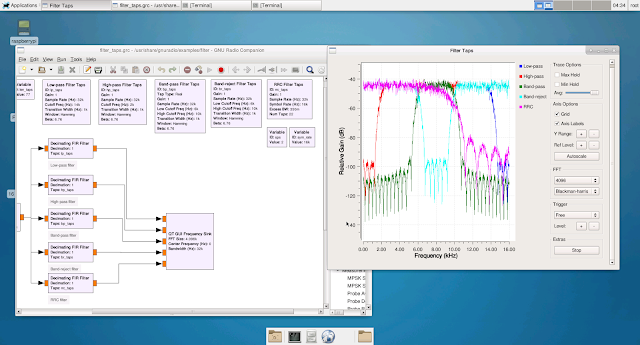
GNURadio Companion Qt Gui Frequency Sync - multiple FIR filter taps sample running on Raspberry Pi 3 custom Linux distribution
© 2018 Bryan R. Hinton

The custom Linux distribution includes support for GNURadio, several FPGA and ARM Powered SDR devices, D-STAR (hotspot, repeater, and dongle support), hsuart, libusb, hardware real-time clock support, Sony 14 megapixel NoIR image sensor, HDMI and 3.5mm audio, USB Microphone input, X-windows with Xfce, Lighttpd and PHP, Bluetooth, WiFi, SSH, TCPDump, Docker, Docker registry, MySQL, Perl, Python, QT, GTK, IPTables, x11vnc, SELinux, and full native-toolchain development support.

The Sony 14 megapixel image sensor with the infrared filter removed can be connected to the Raspberry Pi 3's MIPI camera serial interface. Image capture and recognition can then be performed over contiguous periods of time, and time-lapsed video can be created from the images. With support for Tensorflow and OpenCV, object recognition within images can be performed.

D-STAR hotspot with time-lapsed infrared imaging.
© 2018 Bryan R. Hinton

For the initial run, an infrared Time-lapse Video was created from an initial image capture run of one 3280x2460 infrared jpeg image captured every 15 seconds for three hours. 40, 5mm, 940nm LEDs, powered by 500ma over 12v DC, provided infrared illumination in the 940nm wavelength.

Tensorflow ran in the background (on v4l2 kmod) and provided continuous object recognition and scoring within each image via a sample model. Finally, OpenCV was also installed in the root file system.

The time-lapse infrared video was captured of the living room using the above setup. Below this image are images of Tensorflow running in a terminal in the background on the Raspberry Pi 3 and recognizing/scoring objects in the living room.

Tensorflow running on the Raspberry Pi 3 and continuously capturing frames from the image sensor and scoring objects
© 2018 Bryan R. Hinton
GNURadio Companion running on xfce on the Raspberry Pi 3
© 2018 Bryan R. Hinton

Tuesday, August 16, 2016

Profiling Multiprocess C programs with ARM DS-5 Streamline

The ARM DS-5 Streamline Performance Analyzer is a powerful tool for debugging, profiling, and analyzing multithreaded and multiprocess C programs. Instructions can easily be traced between load and store operations. Per process and per thread function call paths can be broken down by system utilization percentage. Branch mispredictions and multi-level CPU caches can be analyzed. Furthermore, disk I/O usage, stack and heap usage, and a number of other useful metrics can quickly be referenced within the debugger. These are just a few of its capabilities.

In order to capture meaningful information from the DS-5 Streamline Performance Analyzer tool, a Linux, multiprocess, C program was modified to insert 1000 packets into a packet processing simulation buffer. A code excerpt from the program is below. The child processes were modified to sleep and then wake 1000 times in order to simulate process activity. The program was analyzed using the DS-5 Streamline Performance Analyzer tool. There are two screenshots below the code excerpt where the program is loaded into the DS-5 Streamline Performance Analyzer.

void *insertpackets(void *arg) {

   struct pktbuf *pkbuf;
   struct packet *pkt;
   int idx;

   if(arg != NULL) {

      pkbuf = (struct pktbuf *)arg;

      /* seed random number generator */
      ...

      /* insert 1000 packets into the packet buffer */
      for(idx = 0; idx < 1000; ++idx) {

         pkt = (struct packet *)malloc(sizeof(struct packet));

         if(pkt != NULL) {

            /* set the packet processing simulation multiplier to 3 */
            pkt->mlt=...()%3;

            /* insert packet in the packet buffer */
            if(pkt_queue(pkbuf,pkt) != 0) {

               ...
            ...
         ...
      ...
   ...
...

int fcnb(time_t secs, long nsecs) {

   struct timespec rqtp;
   struct timespec rmtp;
   int ret;
   int idx;

   rqtp.tv_sec = secs;
   rqtp.tv_nsec = nsecs;

   for(idx = 0; idx < 1000; idx++) {

      ret = nanosleep(&rqtp, &rmtp);

      ...
   ...
...
ARM DS-5 Streamline - Profiling the process creation application
© 2018 Bryan R. Hinton
ARM DS-5 Streamline - Code View with C code in the top window and ARM assembly instructions in the bottom window
© 2018 Bryan R. Hinton

Source: run.c

Thursday, June 30, 2016

VHDL Processes for Pulsing Multiple GPIO Pins at Different Frequencies on Altera FPGA

DE1-SoC GPIO Pins connected to 780nm Infrared Laser Diodes, 660nm Red Laser Diodes, and Oscilloscope
© Bryan R. Hinton

The following VHDL processes pulse the GPIO pins at different frequencies on the Altera DE1-SoC using multiple Phase-Locked Loops. Several diodes were connected to the GPIO banks and pulsed at a 50% duty cycle with 16mA across 3.3V. Each GPIO bank on the DE1-SoC has 36 pins. Pin 1 is pulsed at 20Hz from GPIO bank 0, and pins 0 and 1 are pulsed at 30Hz from GPIO bank 1. A direct mode PLL with locked output was configured using the Altera Quartus Prime MegaWizard. The PLL reference clock frequency is set to 50MHz, the output clock frequency is set to 50MHz, and the duty cycle is set to 50%. The pin mappings for GPIO banks 0 and 1 are documented on the DE1-SoC datasheet.

Pulsed Laser Diodes via GPIO pins on DE1-SoC FPGA
© Bryan R. Hinton
-----------------------------------------------------------
-- CLOCK A AND B PROCESSES --
-- INPUT: direct mode pll with locked output
-- and reference clock frequency set to 50MHz,
-- output clock frequency set to 50MHz with 50% duty
-- cycle and output frequency scaled by freq divider constant
-----------------------------------------------------------

clk_a_process : process (lkd_pll_clk_a)
begin
    if rising_edge(lkd_pll_clk_a) then
        if (cycle_ctr_a < FREQ_A_DIVIDER) then
            cycle_ctr_a <= cycle_ctr_a + 1;
        else
            cycle_ctr_a <= 0;
        end if;
    end if;
end process clk_a_process;

clk_b_process : process (lkd_pll_clk_b)
begin
    if rising_edge(lkd_pll_clk_b) then
        if (cycle_ctr_b < FREQ_B_DIVIDER) then
            cycle_ctr_b <= cycle_ctr_b + 1;
        else
            cycle_ctr_b <= 0;
        end if;
    end if;
end process clk_b_process;

-----------------------------------------------------------
-- GPIO A AND B PROCESSES --
-- INPUT: direct mode pll with locked output
-----------------------------------------------------------

gpio_a_process : process (lkd_pll_clk_a)
begin
    if rising_edge(lkd_pll_clk_a) then
        if (cycle_ctr_a = 0) then
            gpio_sig_0 <= NOT gpio_sig_0;
        end if;
    end if;
end process gpio_a_process;

gpio_b_process : process (lkd_pll_clk_b)
begin
    if rising_edge(lkd_pll_clk_b) then
        if (cycle_ctr_b = 0) then
            gpio_sig_1 <= NOT gpio_sig_1;
        end if;
    end if;
end process gpio_b_process;

GPIO_0 <= gpio_sig_0;
GPIO_1 <= gpio_sig_1;

Friday, June 3, 2016

FPGA Audio Processing with the Cyclone V Dual-Core ARM Cortex-A9

The DE1-SoC FPGA Development board from Terasic is powered by an integrated Altera Cyclone V FPGA and ARM MPCore Cortex-A9 processor. The FPGA and ARM core are connected by a high-speed interconnect fabric. Linux can be booted on the ARM core and the FPGA and ARM core can communicate.

The DE1-SoC board below has been programmed via Quartus Prime running on Fedora 23, 64-bit Linux. The FPGA bitstream was compiled from the Terasic Audio codec design reference. After the bitstream was loaded on to the FPGA over the USB blaster II interface, the NIOS II command shell was used to load the NIOS II software image onto the chip. A menu-driven, debug interface is running from a terminal on the host via the NIOS II shell with the target connected over the USB Blaster II interface.

A low-level hardware abstraction layer was programmed in C to configure the on-board audio codec chip. The NIOS II chip is stored in on-chip memory and a PLL driven, clock signal is fed into the audio chip. The Verilog code for the hardware design was generated from Qsys. The design supports configurable sample rates, mic in, and line in/out.

Additional components are connected to the DE1-SoC board in this photo. The Linear DC934A (LTC2607) DAC is connected to the DE1-SoC and an oscilloscope is connected to the ground and vref pins on the DAC.

The DC934A features an LTC2607 16-Bit Dual DAC with i2c interface and an LTC2422 2-Channel 20-Bit uPower No Latency Delta Sigma ADC.

3.5mm audio cables are connected to the mic in and line out ports, respectively. The DE1-SoC is connected to an external display over VGA so that a local console can be managed via a connected keyboard and mouse when Linux is booted from uSD.

With GPIO pins accessible via the GPIO 0 and 1 breakouts, external LEDs can be pulsed directly from the Hard Processor System (HPS), FPGA, or the FPGA via the HPS.

Monday, November 9, 2015

Configuring the Altera Cyclone V FPGA SoC Boot loader on a DE0-Nano-SoC board

Understanding the boot loader on a computer system is probably the most important aspect of security. Most computer systems have multiple boot loaders that run in sequence immediately after a power reset is applied to the processor on the computer system. This applies to embedded, desktop, and server systems.

The Altera Cyclone V SoC has an FPGA and a Hard Processor System (HPS) woven into a single processor package. The HPS is a dual core ARM Cortex A9. Building everything from scratch is the best way to figure out how the system works.

The boot sequence on a Cyclone V HPS works like this:

The On-chip ROM (for which source code is not provided) loads the preloader (1st stage bootloader). The preloader then loads U-boot. U-boot then loads the kernel and root file system.

There are two well thought out options for the preloader according to the Cyclone V boot guide. The two options are licensed differently depending on how the source code is built. One is licensed under a BSD license and the other under GPL v2 with U-Boot.

Building a pre-loader image for the DE0-Nano-SoC board was straightforward. Altera provides the bsp-editor utility for customizing the preloader configuration and generating the BSP HPS preloader source code, after which, make is used to build the sources using the Mentor ARM cross toolchain. The preloader settings directory can be found on the DE0-Nano-SoC CD in the DE0_NANO_SOC_GHRD subdirectory.

© Bryan R. Hinton

The preloader load address can be set via the bsp-editor so that the on chip ROM either loads the preloader from an absolute zero address on the sdcard or from a fat partition with id equal to a2 on the sdcard. These are the options for booting from the sdcard.

© Bryan R. Hinton

After the sources are generated and the preloader image is built using the Makefile, U-boot must be compiled. An Altera port of U-Boot is available on github for the Cyclone V FPGA SoC. U-Boot is built using the Linaro ARM cross toolchain.

There's quite a bit that can be done with the Cyclone V FPGA SoC boot configuration. FPGA images can be loaded from U-boot. The jumpers on the board can be configured to boot from the on-board serial flash (QSPI), bare metal applications can be loaded from the preloader, the FPGA can be configured from serial flash, and the list goes on. The HPS SoC Boot Guide for the Cyclone V SoC is a valuable reference and contains all of the boot configuration information.